


Hitachi, in collaboration with Kyushu University, RIKEN, and HREM Research Inc., has announced a revolutionary breakthrough in the observation of magnetic fields at the atomic layer level using their advanced atomic-resolution holography electron microscope. This innovation allows for unprecedented precision in observing magnetic fields within non-uniform samples such as magnetic multilayer films. The implications of this advancement are vast, promising significant strides in materials science and the development of energy-efficient technologies.
The Evolution of Atomic-Resolution Holography
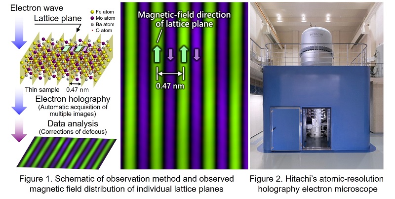
Background and Development
Since 1966, Hitachi has been at the forefront of electron microscopy innovation. The journey began with the development of the holography electron microscope aimed at direct observation of electric and magnetic fields in minute regions. In 2014, Hitachi introduced an atomic-resolution version, and by 2017, they had achieved a resolution of less than 1 nm. The recent breakthrough overcomes previous limitations, enabling the observation of individual lattice planes.
Technical Innovations
Automated Image Acquisition
One of the key advancements is the automated acquisition of over 10,000 high-resolution images within 8.5 hours. This feat enhances the precision of electron holography by leveraging automated control and tuning of the microscope during data collection.
Digital Aberration Correction
Another significant development is the automated correction of minute defocusing through a novel algorithm. This post-image-capture correction process enhances the clarity and resolution of observed magnetic fields, crucial for accurate data analysis.
Applications and Impact
Advancing Fundamental Science
This breakthrough enables detailed observation of magnetic phenomena at the atomic-layer level, providing valuable insights into the behavior of materials and the interfaces within electronic devices. Such precision is essential for advancing fundamental science and developing high-performance magnets and other functional materials.
Towards a Carbon-Neutral Society
The ability to observe and manipulate magnetic fields at such a fine scale holds great promise for creating energy-saving devices. These innovations align with global efforts to achieve a carbon-neutral society by enhancing the efficiency of electronic devices and motors used in various applications, from consumer electronics to industrial machinery.
Collaborative Efforts and Future Prospects
The research was a collaborative effort involving several prestigious institutions, including the National Institute of Advanced Industrial Science and Technology (AIST) and the National Institute for Materials Science (NIMS). The findings were published in the renowned scientific journal Nature, highlighting the significance of this achievement in the scientific community.
Enhancing Technological Capabilities
With the support of the Ministry of Education, Culture, Sports, Science and Technology (MEXT) in Japan, Hitachi’s atomic-resolution holography electron microscope will be utilized by researchers worldwide. This will foster further advancements in various fields, from fundamental physics to cutting-edge electronic devices.
Conclusion
Hitachi’s pioneering work in atomic-resolution holography marks a significant milestone in materials science and technology. By enabling the observation of magnetic fields at the lattice plane level, this innovation opens new avenues for research and development, promising advancements in high-performance materials and energy-efficient technologies essential for a sustainable, carbon-neutral future.